This article addresses the performance of gan and sic power systems in two parts: reliability of gan power devices and stability of sic power devices.
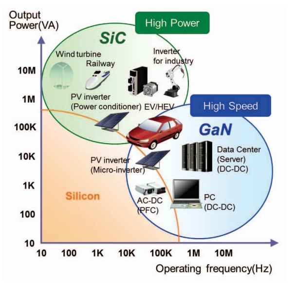
Speaking of effective and reliable alternatives to silicon based devices, silicon carbide (sic) and gallium nitride (gan) are ideal alternatives in applications related to electricity. Sic and gan have unique features of the switch in high-power circuits, making them more efficient and compact. This is achieved by low conductive transistor resistance and high voltage failure in the switch
So far, transistors made of these broadband alkali materials have had working prototypes that demonstrate the best outputs, indicating a great potential for future powerful applications. However, in designing sic and gan designs, engineers still face some problems in understanding the behaviour of switches and thermal control to overcome high power density. Reliability is a factor to be installed in the energy equipment in terms of the future market for chain and system operations.
Reliability of gan power devices
Structural design and problems of transistors gan: in the course of their work, transistors gan use the heterogeneous structure algan/gan for 2d-electronic gas (2deg) with high density of carriers and high mobility of electrons. During this stage there may be many technical difficulties, in particular, the collapse of the current high voltage flow, in which the current of the flow decreases after the application of the current high flow. Eliminating this trap USES removing the electrical field to stop this trap, so the gan sample can be used to analyze the switching system. In addition, transistors gan found application in the commercialization of high-frequency power transistors in cellular base stations. Although the voltage has increased to 50 v, the system can show a smooth transistor operation at higher voltage. Figure 2 shows the current collapse in transistor gan

Reliability of transistors with grid injection: the high concentration of media in algan/gan creates small problems in the operation of transistors gan with constant shutdown. The cave should be introduced from the p-grid to strengthen the formation of electrons in the ditch. This process is called modulation of conductivity. Even in normally switched off transistors, this can lead to low conductivity resistance and high flow currents. Alternatively, transistors with grid injection (git) can be used to resolve this problem by placing p algan grids at heterogeneous crossings. At the same time the channel is completely exhausted under the closure. The low ronqg (RON: resistance, qg: grid charge) with 700nc is one-third smaller than the modern silicon moose supertransition, and has a much higher potential for high-speed switches. Pulse voltage measurement (i-v) is used to describe the collapse of the git current on the si background. Use the grid voltage in the off and zero displacement, as well as very short leakage impulses. Figure 3 shows the git cross section diagram.

Reliability of propulsion devices sic
Sic structural design and transistor problems: installation of the sic power device on the sic substrate using the crystal on the eccentric substrate and the improved mass of the sic extensible membrane. Systems used for mass production are configured with double diffusion mosfet (dmos). This is usually used for existing si mosfet capacities. One of the main drawbacks of sic transistors is that after applying a high positive or negative voltage. This can damage the reliability of the transistor sic and eventually disrupt the operation of the device. When applying high grid voltage, the captured electron/hole depends on the grid voltage pole. This leads to a change in the threshold voltage. Another reliability problem may be degradation of stereodydes based on pn-transition. This begins as soon as the plane of the foundation begins to form, so a better quality of extensivity is required.

Diode integrated mosfet (diomos) and reliability: to eventually reduce the cost of the chip in sic switches, diode integrated mosfet semiconductor (diomos) is offered.
As shown in figure 4, diomos has an additional outer layer of the channel formed under the grid insulation. Using the channel layer as a reverse current path, the integral diode is not subjected to reverse current. Under the diomos grid, the thin trench outer layer with heavy n alloying reduces the electronic barrier to 0.8 ev. This is crucial for adjusting the device to reverse conductivity. When observing the properties of diomos i-v, it was discovered that the reverse diode has a low built-in voltage. In addition, the threshold voltage shifted from positive to 15v and negative to 15v has not changed. Since diomos has stable properties of up to 1000 hours, diomos can be used in real switch applications with sufficient reliability.
Conclusions and recommendations
Summing up the traditional devices and their reliability, the most modern devices with power switches gan and sic developed by panasonic were discussed. The use of sic diomos, which includes reverse diodes, can reduce the total cost of the chip for the system. After applying a high pressure grid displacement and completing the degradation of the volumetric diode, there is a stable operation without moving the threshold voltage.
Demonstration propulsion devices consisting of sic and gan have been tested for high temperature reverse displacement. The tests lasted more than 1,000 hours, which makes them promising for improving the efficiency of electric power switching systems in the electronics industry in the future.

 BOM
BOM RFQ
RFQ